

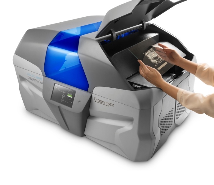
Israel-based company Nano Dimension has filed a patent application with the U.S. Patent and Trademark Office for simultaneously curing and sintering of two types of ink. A conductive metal ink and an insulator ink will be used for 3D printing electronics circuits.
According to Nano Dimension, the new technology has the potential to reduce the number of critical systems in a printer and thus allows for a significant reduction in the production costs of the printer, increased printing speed, system miniaturisation and increased overall system reliability.
The current standard curing and sintering approach uses a number of different systems to cure and sinter the inks. Each such system adds cost and complexity, while this new approach has the potential to reduce both.
The unique chemical structure of the inks developed by the company’s in-house laboratory consist of nanoparticles to absorb radiant energy, causing a plasmonic effect on the surface of the nanoparticle. The plasmonic waves are immediately converted into heat, which causes the fusion of silver nanoparticles due to the high surface energies at the nanoscale. This sintering process results in a final uniform metallic trace.
The photoinitiated insulating ink absorbs the radiation emitted by the advanced 3D printer’s integrated process system and solidifies instantly. Once cured, the insulating ink demonstrates mechanical strength and high thermal resistance.
Subscribe to our Newsletter
3DPResso is a weekly newsletter that links to the most exciting global stories from the 3D printing and additive manufacturing industry.