

Prototypes for new printed circuit boards (PCBs) created with EOS technology
At the beginning of 2016, many people were writing about the end of Moore’s Law, anticipating that the performance of computer chips would no longer be doubling every two years. The reason for this is that the structures on the processors themselves are already within a few nanometers of what is possible. Further reductions are almost impossible from a technical point of view. In order to continue improving performance, manufacturers are working on the architecture, which stacks multiple structural layers on top of one another. A similar approach has already been established within the field of circuit carriers. The German firm of Beta LAYOUT GmbH has successfully harnessed EOS technology to manufacture and test the prototypes for these innovative carriers.
Challenge
Circuit carriers and traditional PCBs have always been a little overshadowed by the microprocessors that operate on them. This is somewhat unjust because, of course, having the best brain is of little use without the benefits of a high-performance central nervous system. It’s a similar story in the microelectronics sector: almost all contemporary devices require a circuit board in order to incorporate one or more chips, plus the additionally required electrical components. This creates a network that fulfills a range of tasks, from supplying of electricity, circuitry, through to the output of signals.
In new devices, there is often only a very small amount of installation space available for conventional circuit boards. One reason for this is that a lot of electronic equipment is becoming ever smaller; and even when the form itself is larger, there tends to be very little space left over for the actual electronics. The existing volume is required for housing screens, for example, more and more interfaces and output points, as well as larger batteries. The time when a simple lab PCB was sufficient for the experimental construction of new circuitry are now, in most cases and most sectors, long gone. Alongside the available installation space, weight is a key factor – compact, three-dimensionally constructed circuit boards also have an important role to play here.
With contemporary electronic products, the circuitry often has to compete for the limited space within the housing. When conventionally stacked, PCBs can no longer accommodate all of the necessary components, so that the aforementioned three-dimensional circuit carriers become the solution of choice. Here again, the ever-shorter life cycles of many devices pose additional challenges: injection molding is far too expensive to manufacture prototypes. For this reason, Beta LAYOUT GmbH decided to search for a cheaper, high-performance alternative.
Solution
There is no technology better suited to the demands of multi-layer architecture than additive manufacturing. This is because it uses a laser to build up a component, layer by layer. This is why Beta LAYOUT relies on the technology and uses plastic parts manufactured by 3D printing. The innovation takes place after the printing process itself; once they’ve been made, the models are coated with a special finish that is furnished with an additive. The subsequent so-called ‘laser direct structuring’ (LDS) generates layouts, which can be turned into conductor tracks by activating the finish.
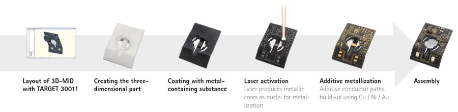
The laser triggers a physical-chemical reaction that creates metallic spores while simultaneously roughening the surface. After laser direct structuring, the models are placed in a copper bath free of electric current. There, copper particles are deposited on the previously activated areas to create conductor tracks. After copper coating, the conductor tracks can undergo further copper plating through galvanization, or be directly furnished with a surface finish. After this, Beta LAYOUT then adds the individual components to the unit in the company’s internal assembly department. The finished pieces serve as initial prototypes and models, allowing function testing and a check of design layouts.
“We offer manufacturing of 3D-MID (mechatronic integrated devices) as prototypes for diverse companies,” explains Manuel Martin, Product Manager 3D-MID at Beta LAYOUT GmbH. “Working with EOS’ FORMIGA P 110, we are in a position to deliver high-quality products to our customers fast. What’s particularly practical in all this is that we are even able to deal with orders of 3D models via websites and online shops. Additive manufacturing has enabled us to successfully expand our business model.”
Results
Whether for individual developers or large established companies, additive manufacturing ensures that custom-made circuit carriers can be used for the prototypes of new electronic devices. The plastic components can be produced quickly and at an attractive price. The process simultaneously offers the nessary level of precision and high component-quality, allowing the required basic body to be manufactured as if it were already a close-to series product – an aspect that should not be underestimated, particularly with test runs.
The EOS technology also provides a high degree of flexibility: the machine used is able to process various materials, including, for example, PA 3200 GF which is filled with glass beads, or the aluminum-filled polyamide Alumide. High-performance polymers such as PEEK and various metals are also available. The crucial point is that all the materials are capable of withstanding high temperatures, a limitation of the injection-molding process in series production. Because of this flexibility, Beta LAYOUT is able to fulfill the various individual requirements of its customers, for example, by responding to the particular characteristics of the intended purpose of the circuit carrier. In this way, the company can develop individual, optimized solutions, be this in terms of lower costs, a higher degree of temperature resistance, or any other specific requirements.
Besides these advantages, additive manufacturing also offers another additional bonus:
“Ultimately, what we are experiencing here is a democratization of advanced technology. Without innovations such as this, we would not be able to offer 3D-MID as a service at all,” says Manuel Martin. “This would mean that many smaller companies and development houses would have no chance of realizing such prototypes. Consequently, the much talked-about innovation and creative power of small and medium-sized companies would lose momentum and the research and development sector would be a lot less dynamic.”
Additive manufacturing is a catalyst for further innovation– and, in this way, perhaps a point of departure towards establishing a new Moore’s Law.
Manuel Martin, Product Manager 3D-MID, Beta LAYOUT GmbH:
“Thanks to its many advantages, additive manufacturing technology offers high added value for a broad range of market participants. Research and development profits through our services, which, in turn, has a positive impact on our business model. This enables us to offer the benefits of advanced technology to a large number of users.”
Subscribe to our Newsletter
3DPresso is a weekly newsletter that links to the most exciting global stories from the 3D printing and additive manufacturing industry.