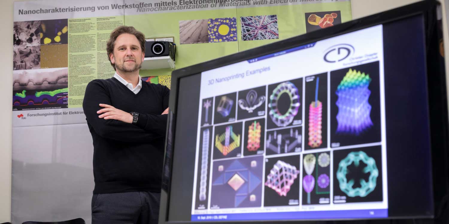
The shape, size and optical properties of 3-dimensional nanostructures can now be simulated in advance before they can be produced directly on a wide variety of surfaces with high precision.
For around 20 years, it has been possible to apply nanoparticles to surfaces in such a way that they concentrate or manipulate light in a desired way or trigger a reaction. Such optically active nanostructures can be found in solar cells and biological or chemical sensors, for example. In order to expand their range of applications, researchers at the Institute of Electron Microscopy and Nanoanalytics at TU Graz and the Center for Electron Microscopy (ZFE) have been working for over ten years on producing not only flat nanostructures, but also complex, free-standing 3D architectures. The team led by Harald Plank, Verena Reisecker and David Kuhness has now achieved two breakthroughs. They are able to precisely simulate the desired optical properties as well as the required shape and size of the nanostructures in advance and produce them precisely on the basis of the simulation. They are also able to remove chemical impurities that arise during production without affecting the 3D nanoarchitectures.
Trial-and-error process becomes superfluous
Until now, three-dimensional nanostructures required a lengthy trial-and-error process until the product had the desired optical properties. This effort is now finally a thing of the past. “The agreement between our simulations and the real plasmonic resonances of a wide range of nanoarchitectures is very high,” explains Harald Plank. “This is a huge step forward. The hard work of recent years has paid off.” The technology is currently the only one in the world that allows complex 3-dimensional structures with shaped elements smaller than 10 nanometers to be produced directly and in a controlled manner on almost any surface. By comparison, the smallest viruses are 20 nanometers in size. “The biggest challenge in recent years has been the transfer of 3D architectures into high-purity materials without destroying the morphology,” explains Harald Plank. “This leap in development enables new optical effects and application concepts thanks to the 3D aspect.” Probes or optical tweezers with sizes in the nanometer range are now within reach.
Precisely controlled electron beam
The researchers use focused electron beam deposition (focused electron beam induced deposition) to produce the nanostructures. In this process, the relevant surface is coated with special gases under vacuum conditions. A finely focused electron beam splits the gas molecules, whereupon parts of them change into a solid state and adhere to the desired location. “By precisely controlling the beam shift and exposure time, we are able to produce complex nanostructures with lattice or sheet-like structural elements in a single step,” explains Harald Plank. By layering these nanovolumes on top of each other, three-dimensional structures can ultimately be constructed.
This research is anchored in the Field of Expertise “Advanced Materials Science“, one of five strategic research focuses at TU Graz.
Publication: Spectral Tuning of Plasmonic Activity in 3D Nanostructures via High-Precision Nano-Printing. Advanced Functional Materials, November 1, 2023 (DOI: https://doi.org/10.1002/adfm.202310110).
Authors: Verena Reisecker, David Kuhness, Georg Haberfehlner, Michele Brugger-Hatzl, Robert Winkler, Anna Weitzer, David Loibner, Martina Dienstleder, Gerald Kothleitner, Harald Plank
Subscribe to our Newsletter
3DPresso is a weekly newsletter that links to the most exciting global stories from the 3D printing and additive manufacturing industry.


