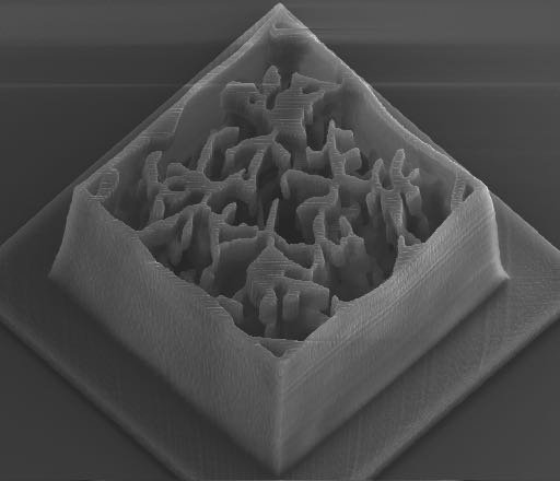
A new technology developed at Caltech allows researchers to “engineer” optical devices and then print them out using a special 3D printer. These devices are made of so-called optical metamaterials, which derive their properties from structures so small they are measured in nanometers, and they could allow cameras and sensors to detect and manipulate properties of light in ways that were previously impossible on a small scale.
“Generally, most of these things are done in a thin layer of material. You take a very thin piece of silicon or some other material and you process that to get your device,” he says. “However, [the field of] optics lives in a three-dimensional space. What we are trying to investigate here is what is possible if we make three-dimensional structures smaller than the wavelength of light that we are trying to control.”
To demonstrate, Faraon’s lab has developed tiny devices that sort incoming infrared light by both wavelength and polarization. The researchers hope to develop similar devices for the visible light range and for use in cameras and VR spaces.
The devices have an organic, chaotic structure that is achieved through constant design optimization using an algorithm. Gregory Roberts, lead author of the study, compares the process to breeding a good sheepdog.
“The design software at its core is an iterative process,” Roberts says. “It has a choice at every step in the optimization for how to modify the device. After it makes one small change, it figures out how to make another small change, and, by the end, we end up with this funky-looking structure that has a high performance in the target function that we set out in the beginning.”
Faraon adds: “We actually do not have a rational understanding of these designs, in the sense that these are designs that are produced via an optimization algorithm. So, you get these shapes that perform a certain function. For example, if you want to focus light to a point—so basically what a lens does—and you run our simulation for that function, you most likely will get something that looks very similar to a lens. However, the functions that we are targeting—splitting wavelengths in a certain pattern—are quite complicated. That’s why the shapes that come out are not quite intuitive.”
To translate the designs into physical devices, the researchers used two-photon polymerization lithography (TPP), a form of 3D printing that selectively cures a liquid resin with lasers.
Faraon says the work is a proof of concept, but that with a little more research, a practical manufacturing process could be developed.
The work, titled “3D-patterned inverse-designed mid-infrared metaoptics,” is published in the April 14 issue of Nature Communications. Other co-authors include Conner Ballew, formerly at Caltech and now at JPL, which Caltech manages for NASA; Tianzhe Zheng, a Ph.D. candidate in applied physics; Sarah Camayd-Muñoz, formerly at Caltech and now at Johns Hopkins University; and Juan C. Garcia and Philip W. C. Hon of Northrop Grumman.
Funding for the research was provided by the Defense Advanced Research Projects Agency (DARPA), the Rothenberg Innovation Initiative, the Clinard Innovation Fund at Caltech, and the Army Research Office.
Subscribe to our Newsletter
3DPresso is a weekly newsletter that links to the most exciting global stories from the 3D printing and additive manufacturing industry.


